Non-standard RGB video conditioner
RGB video input for Altera DE1 board + PAL Modulator
This is an experimental video capture project. The goal is to capture poorly modulated RGB + Sync signal as produced by an old Soviet home PC, detect sync, massage the signal levels, insert correct sync pulses, add PAL colour modulation and output a signal that would be acceptable by a modern colour TV.
Вектор-06ц is the particular computer that I had in mind. Its video generation circuit is infamous for blatant disregard of all existing video standards at once, which makes it rather difficult to connect it to modern monitors and televisions.
Outline
The main platform is Altera DE1 FPGA board. It is fairly outdated, but it's the one that I have on my bench. Going up to more modern FPGA kits is easy.
A working PAL modulator that works well in my vector06cc FPGA replica of the same computer already exists.
To sample RGB + Sync video signal one needs a decent speed ADC, preferrably with 4 channels, or a special video capture chip. I found nothing that would suit the job easily available. However, I found out about a neat trick of using LVDS input pairs available on FPGA chips to implement custom sigma-delta ADC. No need for special chips!
The basic working principles of such ADC are described in the paper called "Leveraging FPGA and CPLD digital logic to implement analog to digital converters" by Ted Marena. There's also an excellent explanation and demonstration of the principle in One Bit ADC video by Jeri Ellsworth.
Block diagram
Here's a simplified diagram of the project:
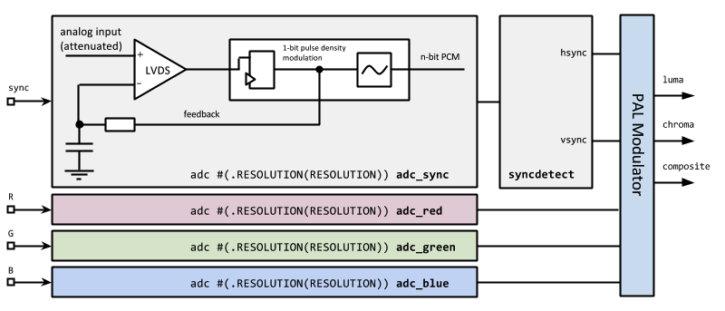
The video signal comprised of H+V composite sync and R, G, B signals is level-shifted to be within range of LVDS inputs (see schematic) and is fed into the ADC. The ADC modules feed back the resulting PDM signal to the negative side of LVDS inputs, and to the input averaging filter. The recovered PCM signal is formed on the output of the filter. There are variations of input filters in the source code.
The recovered sync signal is passed to the input of sync detector module, which tries its best to recover horizontal and vertical sync pulses. It's designed to be able to cope with bizarre sync signals produced by bizarre computers. It does the job with variable success. Usually the problems are of electrical rather than of logical nature. For example, Вектор-06ц is known to have no equalization pulses, which results in huge amplitude jumps during vertical sync or even simply empty lines.
The resulting sync, R, G, B signals are fed into the video generator module. It consists of sync generator and PAL modulator. The outputs are chroma, luma and mixed CVBS composite signals. They are output either using primitive linear DAC on VGA connector of DE1 board, or using a sigma-delta modulator. The latter allows for having separate luma + chroma (S-Video) signals on the output.
Generating output
S-video using a sigma-delta DAC is very simple:
reg [DAC_RESOLUTION:0] ydac;
reg [DAC_RESOLUTION:0] cdac;
always @(posedge clk_out)
begin
    ydac <= ydac[DAC_RESOLUTION-1:0] + tv_luma[RESOLUTION-1:RESOLUTION-DAC_RESOLUTION];
    cdac <= cdac[DAC_RESOLUTION-1:0] + tv_chroma[RESOLUTION-1:RESOLUTION-DAC_RESOLUTION];
end

assign GPIO_0[10] = ydac[DAC_RESOLUTION];
assign GPIO_0[11] = cdac[DAC_RESOLUTION];
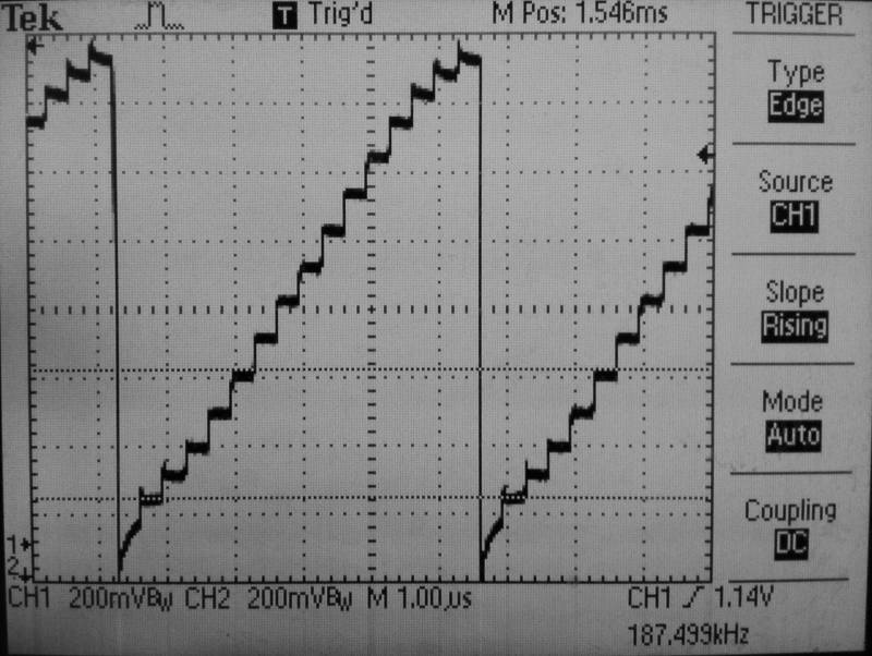
Linear DAC on VGA pins of DE1 board is more interesting. The resistor DAC on DE1 allows 4 bits per channel, or just 16 levels. This is not a lot for composite analog video. Here's what a saw waveform looks like if only 4 bits are used:
However with a little bit of magic, described in detail in my article here, it is possible to get much higher resolution from this DAC. Here's an example:
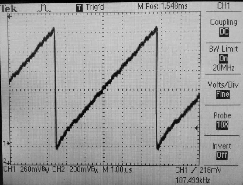
The magic DAC is implemented using a look-up table:
dactable dactaklakpak(.address(tv_cvbs), .clock(clkpalFSC), .q(dacval));
assign VGA_R = dacval[3:0];
assign VGA_G = dacval[7:4];
assign VGA_B = dacval[11:8];
Project files
- hw contains KiCad files for the DE1 addon board. Check out the schematic.
- iverilog contains simulation of video signals as produced by BK-0010, and their detection
- src Altera Quartus II project and synthesizable core
Results
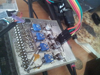
The input board looks like this:
Single channel, B&W+Sync only with BK-0010:
Single channel passthrough from C64. Signal sampled and output on DE1 VGA pins without any conditioning. Image credit: Deus ex Machina by Crest/Oxyron.

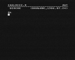
RGB+Sync from Vector-06c, internally PAL modulated in FPGA (captured by TV tuner)

Work log on a forum (in Russian)
Conclusion
This is a research project and I never made it into a finished box with just power plug and connectors. It works, but is not perfect. The results on my monitor are acceptable. There were some problems with PAL encoding that I could not resolve that I observed on a couple of older TV sets. They are not related to the main focus of the project however: sampling video signals using nothing but a few LVDS pins.
It is definitely possible to capture low-spec video signals with a 10 year old FPGA using only a few additional discrete components. The practical aspects of this depend on the situation. Where reliability matter and source signal is known to be within the specifications, a dedicated chip like TVP7002 would most likely do better. One interesting example of a project that uses TVP7002 is Grabor. But with a such chip I would not be able to extract nonstandard video signal from Вектор-06ц, just like my monitor cannot do that. Where flexibility and fine control is required, being able to implement video decoding on the lowest possible level can be beneficial.
The quality of input suffers from quite a bit of noise. I believe part of this is due to really long electrical connections that are hard to shorten because of the way the connectors on the board are done. In case of practical application it should be possible to improve the noise characteristics by implementing the inputs using shorter, carefully layed out trace pairs, hopefully reducing parasitic capacitance of the connections, thus allowing higher sampling frequency. Finding an optimal configuration of PCB layout for such application would be an interesting project in itself.
References
- Leveraging FPGA and CPLD Digital Logic to Implement Analog To Digital Converters LatticeSemi Whitepaper
- Simple Sigma-Delta ADC LatticeSemi RD1066
- FPGA RGB2VGA scan doubler project by Felipe Antoniosi uses LVDS inputs to implement a successive approximation ADC
2014-2015 Viacheslav Slavinsky, http://sensi.org/~svo