FPGA-TX
FPGA-TX is an FPGA based radio transmitter, that can transmit at frequencies up to 400MHz. So far, FPGA-TX supports AM, FM, LSB, USB, Wideband FM, and Wideband FM Stereo.
FPGA-TX has been tested on Ubuntu, but it uses portable libraries, so could be ported to other platforms with a little effort.
Before you transmit, know your laws. FPGA-TX has not been tested for compliance with regulations governing transmission of radio signals. You are responsible for using FPGA-TX legally.
FPGA-TX was inspired by the Raspberry Pi FM transmitter and rpitx projects. FPGA-TX provides a similar capability but uses FPGA based hardware to generate a modulated output using GPIO pins.
Software
Python Modules
FPGA-TX has some dependencies on Python modules. The software uses the sox tool to provide a portable and flexible method for capturing/reading audio.
sudo apt-get install python-numpy python-scipy python-serial python-wxgtk3.0 python-matplotlib sox git
Serial Port Permissions
To run tx as an ordinary user, you need to grant read and write access to the appropriate serial device. A convenient way to achieve this on Ubuntu based systems is to add yourself to the dialout group.
sudo usermod -a -G dialout $USER
Install
git clone https://github.com/dawsonjon/FPGA-TX.git
cd FPGA-TX
sudo python setup.py install
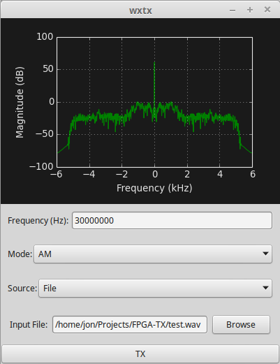
GUI transmitter (wxtx)
wxtx
Command line utility (tx)
tx -f=<frequency> -m=<mode>"
Accepts data from stdin in mono raw 16-bit pcm format
Options
-f=<frequency>
Specify transmit frequency in Hz
-m=<mode>
Mode may be AM or FM
-d=<device>
specify USB/serial device of transmitter. default is /dev/ttyUSB1
Examples
####transmit narrow band FM on 12MHz
sox test.wav -t raw -b 16 -r 12k - | tx -f=12e6 -m=fm -r=12000
####transmit stereo FM on 88 MHz
sox myfile.mp3 --channels 2 -t raw -b 16 -r 48k - | tx -f=88e6 -m=stereo -r=12000
####transmit lower sideband on 10 MHz (using soundcard input, e.g. microphone)
rec -t raw -b 16 -r 12k - | tx -f=10e6 -m=lsb
FPGA Firmware
Install Python Modules
sudo apt-get install python-numpy python-scipy python-serial
Install Chips-2.0
You will need Chips-2.0 to build the FPGA embedded C code.
git clone --recursive https://github.com/dawsonjon/Chips-2.0.git
cd Chips-2.0
sudo python setup.py install
cd ..
Install Additional software
Requires the vendor's tools for the target FPGA card. Vivado webpack edition can be downloaded from the Xilinx website. You will need to edit the fpga_tx/user_settings.py file to point to the location where Vivado is installed.
Clone the git repo
git clone https://github.com/dawsonjon/FPGA-TX.git
cd FPGA-TX
Compiling the C code
This step is optional, you can use the pre compiled files.
./run_fpga cmod_a7_15 compile
Building the VHDL and Verilog into an FPGA bitstream
This step is optional, you can use the recompiled files. You can also replace nexys_4 with cmod_a7_15 depending on the target platform.
./run_fpga cmod_a7_15 compile build
Download the bitstream into FPGA (volatile)
Do this step if you want to try out the FPGA firmware without overwriting the SPI PROM. The FPGA will lose its configuration each time it loses power.
./run_fpga cmod_a7_15 compile download
Download the bitstream into SPI Flash (non-volatile)
Do this step if you want to program the SPI PROM on the FPGA card. The FPGA will retain its configuration if power is lost.
./run_demo cmod_a7_15 compile flash
Technical Details
Hardware
###FPGA Dev kit
At present, two development cards are supported, the Digilent Nexys 4 was used in the initial experiments, but the Digilent CMOD A7 (the 15T version) is cheaper, doesn't have so many unnecessary peripherals, has a more convenient USB-dongle form factor, and makes a good basis for a transmitter project.
###Transmitter Prototype
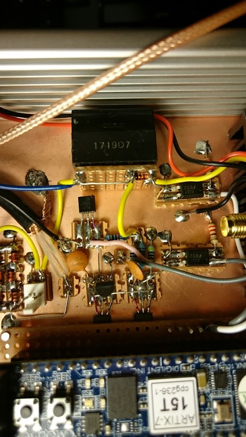
After some initial experiments had been made to establish that the popular transmission modes could be synthesised in software, a prototype transmitter was built to demonstrate that the FPGA could be incorporated into a self contained communications transmitter.
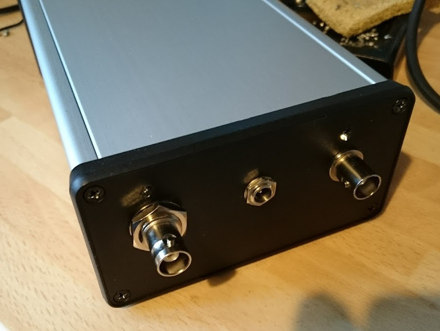
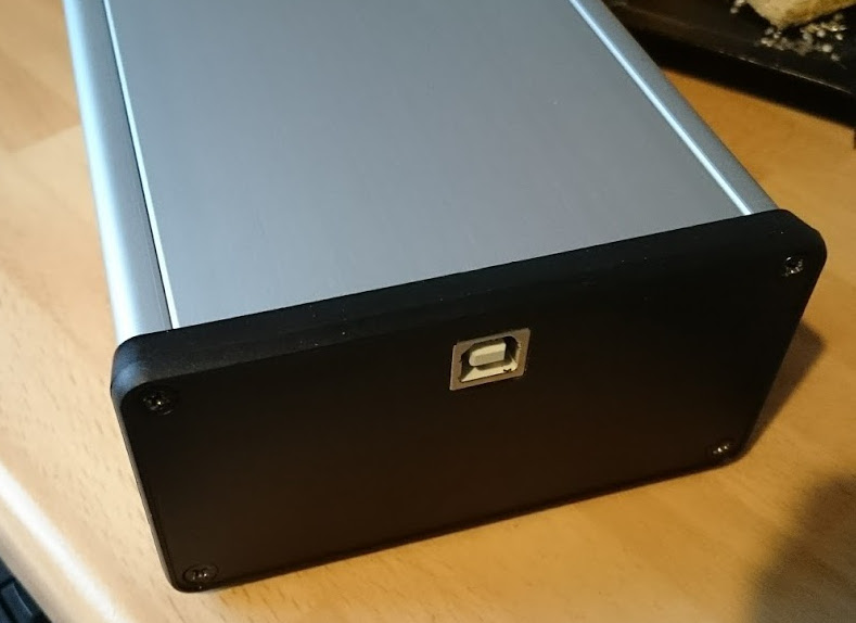
The transmitter prototype consists of an FPGA module to act as a controller and modulator, a small wideband RF Power Amplifier, and circuitry to allow an antenna to be switched between transmit and receive modes.
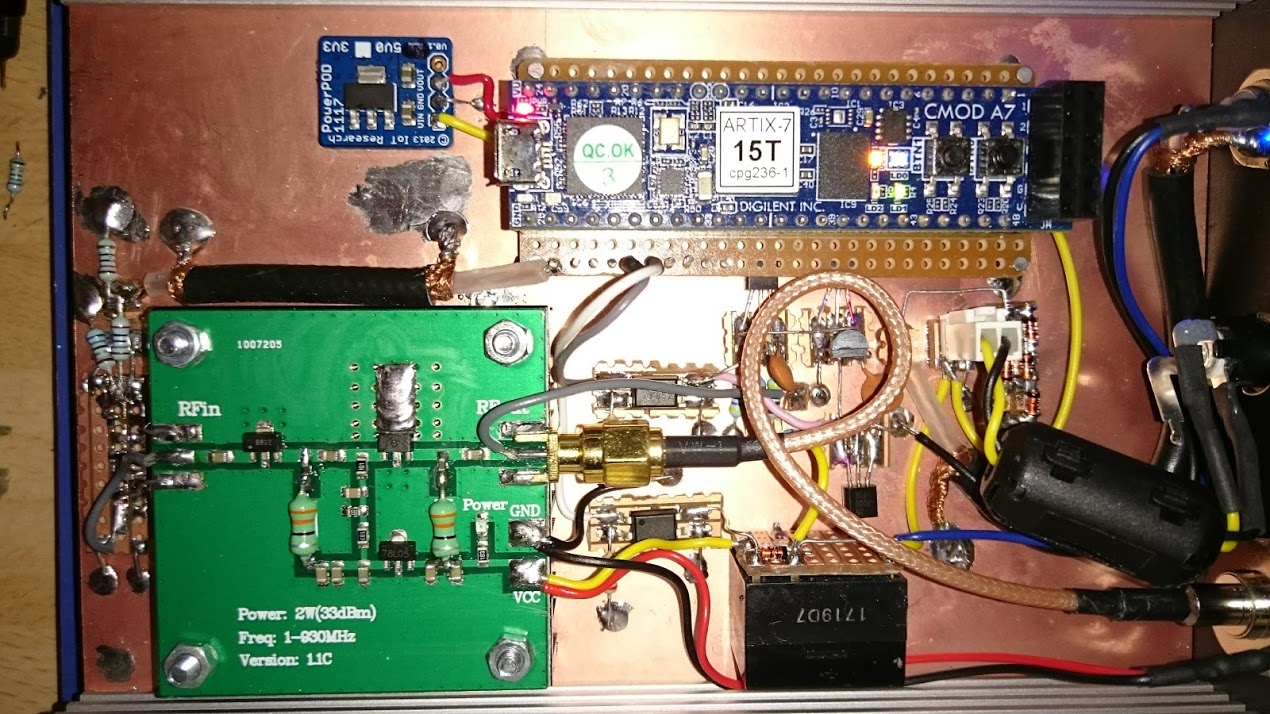
The prototype requires an external 12v power supply to provide sufficient power for the RF amplifier. When operating the CMOD A7 under USB power, programming of the flash was unreliable. To overcome this, a diode was removed from the CMOD, and an external 5V siwtching regulator was used to power the CMOD. This resulted in much more reliable flash programming. The first regulator had an 800mA rating and it got rather hot, I replaced this with a 3A module which doesn't even get warm.
###Amplifier
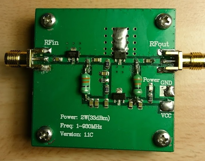
The first experiments were conducted without an amplifier using a very short length of wire attached to a PMOD connector, allowing test signals to be picked up a few feet away. To build a more powerful transmitter a small inexpensive 2 watt broadband amplifier was purchased on e-bay for use in the transmitter prototype.
###Attenuator
The FPGA pin is configured to provide an 3.3v LVTTL output with the maximum drive strength of 24mA. Assuming that the LVTTL output can source 24mA and a 2.0V swing, the output impedance of the FPGA is assumed to be approximately 80 ohms.
With a pk-pk voltage swing of 2V, the RMS voltage swing for a sin wave is approximately 0.7V. With a load impedance of 80 ohms, the RMS power can be estimated to be 6.25 mW, or about 8dBm. The wideband amplifier has an input impedance of 50 ohms, and has a maximum input power of 0dBm. An attenuation of 15dB was chosen to allow some margin.
A pi attenuator was designed using an online calculator. Resistance values of 120 ohms, 68 ohms and 180 ohms were selected for the input, output and series resistor respectively.
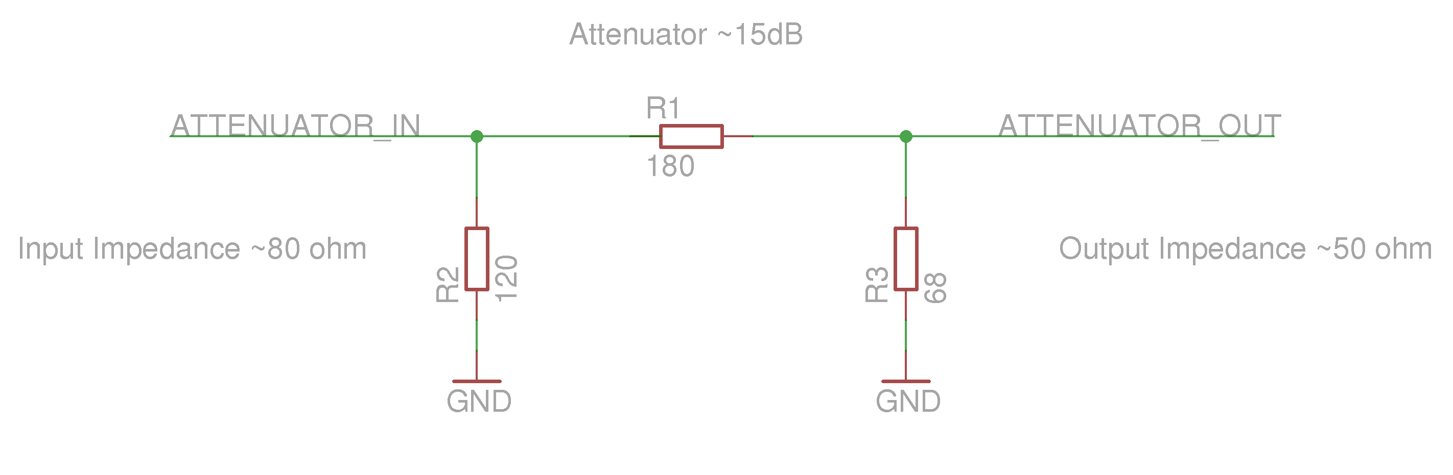
In the prototype the filter is constructed using through hole resistors.

###Filter
In the digital domain, dithering has been used to minimise the harmonic and spurious signals within the band of interest (0-400MHz). The harmonics a spurious signal power has not been removed, but spread evenly across the band in the form of wideband noise.
There is nothing that can be done in the digital domain to remove harmonic and spurious signals outside the band. For this reason, low pass filter with a cut-off frequency of 400MHz is added before the amplifier.
An online calculator was used to calculate the component values for a fifth order Chebyshev filter with 1dB passband ripple and an impedance of 50 ohms.
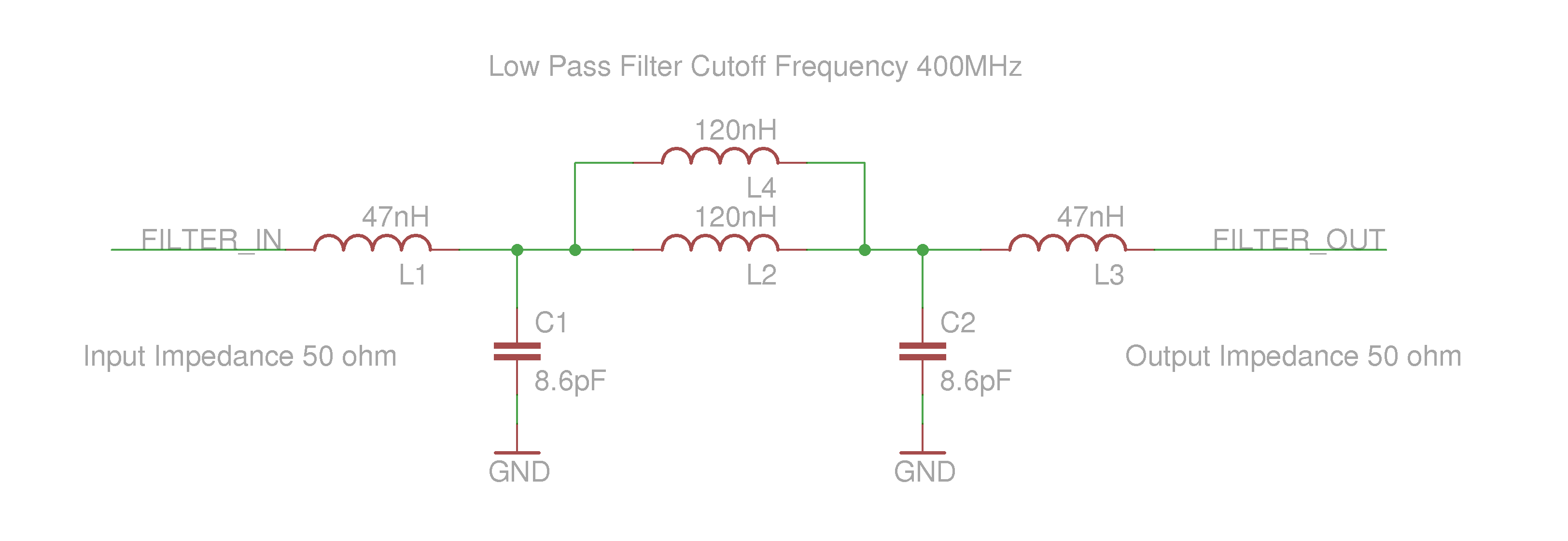
In the prototype, the surface mount capacitors and inductors can only just be made out.
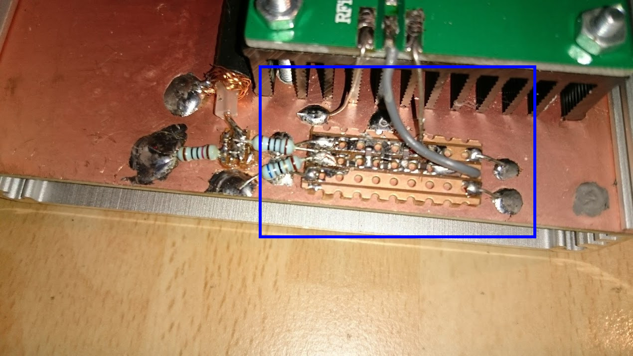
###TX/RX Switching
The FPGA module provides two signals to switch between RX and TX modes, TX_PA turns the amplifier on and off, TX_RX connects and disconnects the receiver from the antenna. The transmitter is permanently connected to the antenna.
Each signal is fed through an opto-isolator. The TX_PA signal turns on a relay supplying 12V to the power amplifier. TX_RX controls 2 MOSFETs, one connects or isolates the receiver, the other shorts the receiver connection during TX mode. In addition, signal diodes prevent large signals reaching the receiver. A 3rd MOSFET simply acts as an inverter.
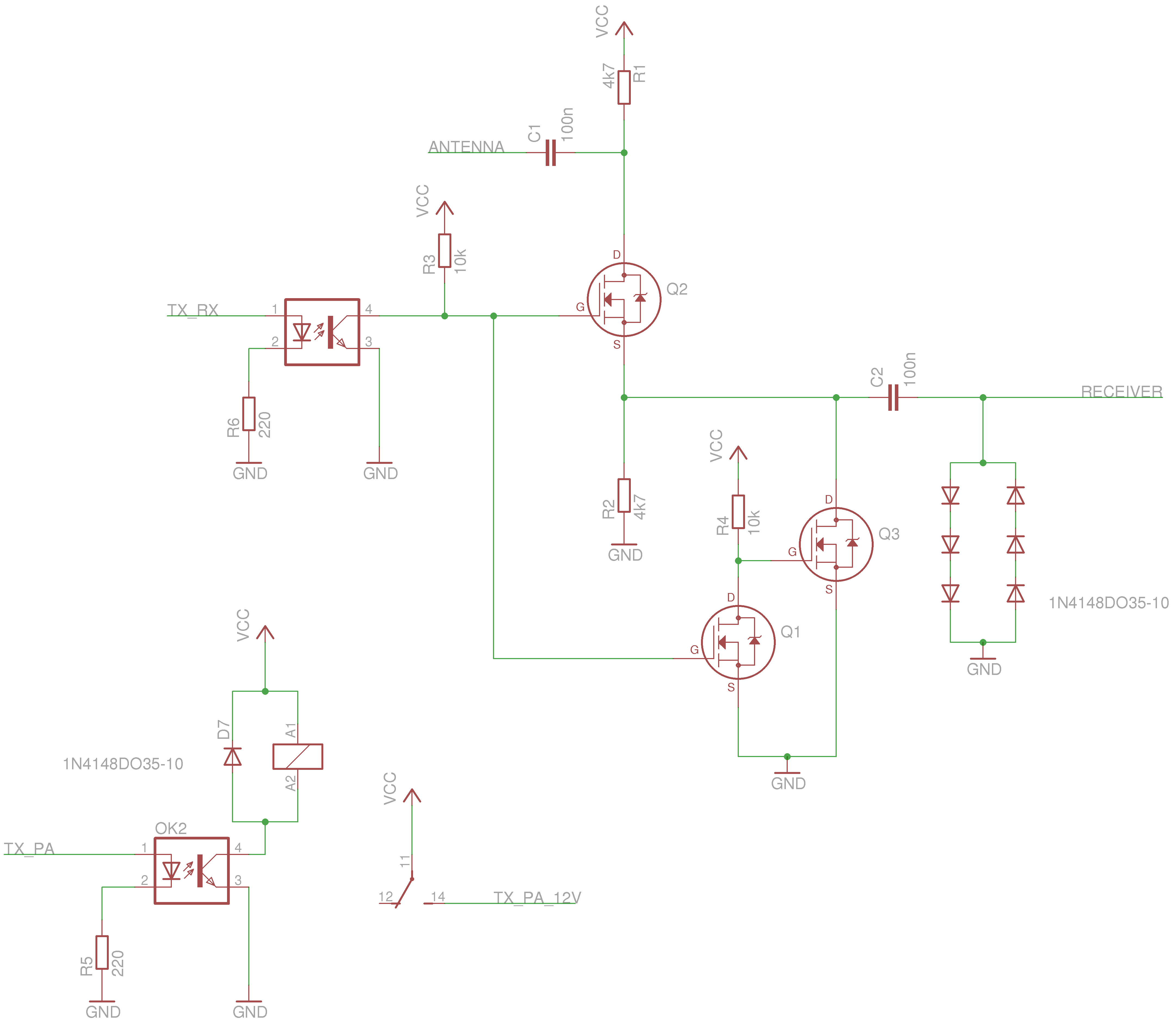
The MOSFET circuit is based on this tx rx switch. The prototype switch is shown below.
The FPGA sequences the control signals to allow for any
delay in the relays switching the power amplifier, and ensures that the
receiver is always isolated while the power amplifier is switching on and off.
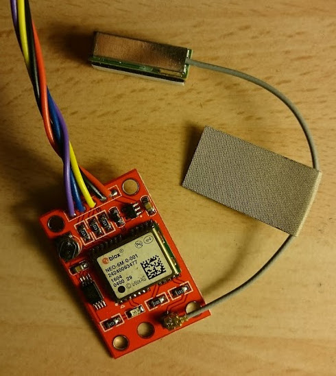
###GPS Calibration
The crystal oscillators used in FPGA development cards typically have an accuracy of the order +/- 100 ppm. At a frequency of 400MHz, this would give an error of +/- 40KHz which is clearly not acceptable when communication channels are typically 12.5KHz wide.
One possibility would be to use a more accurate external oscillator,Temperature Controlled Crystal Oscillators (TCXOs) are available with accuracies of around +/-0.1ppm.
An other possibility is to make use of low cost GPS modules. These provide a reference signal with a tightly controlled period of 1 second. A counter within the firmware allows us to measure the number of 100MHz clock cycles that occur during each 1 second pulse. This gives us a method of measuring how fast or slow the clock is running, and allows us to calculate a correction to the commanded frequency.
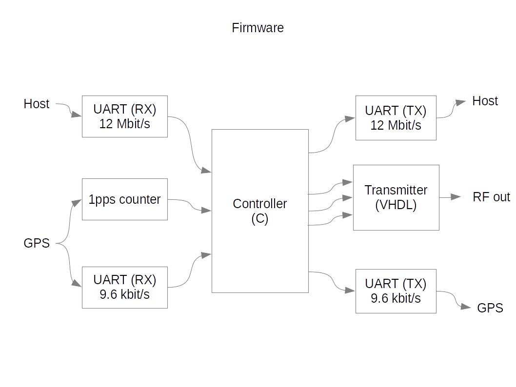
FPGA Firmware
The FPGA firmware consists of 2 major parts, the transmitter written in VHDL, and the Controller written in C (using Chips to convert to Verilog).
The Transmitter
The transmitter allows both Quadrature Amplitude Modulation, and Frequency modulation. The sample rate is 800 MHz, while the clock rate is 100 MHz, in each clock cycle, 8 samples are processed. In general, this is achieved by implementing 8 parallel data paths.

NCO
The NCO is based on a 32 bit accumulator which generates the phase, the phase is fed into a lookup table of sin or cosine values. A 32 bit accumulator gives a resolution 0.186 Hz with an 800 MHz Sample Rate.
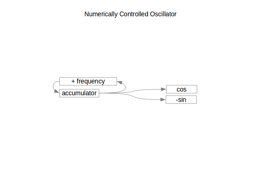
However, since we are working at a sampling frequency of 800 MHz, with a clock frequency of 100 MHz, it is necessary to calculate the next 8 output samples each clock cycle. The sequence should be: accumulator, accumulator + frequency, accumulator + 2 * frequency, .., accumulator + 7 * frequency. Since multiplication by a power of 2 is a much cheaper operation, a tree can be employed to calculated these values using shifts and adds. The logic paths can easily be broken using pipeline registers, so long as the feedback loop only has a one clock cycle latency.

Interpolate
The Interpolate block increases the sample rate of the I/Q data by 65536. With an output sampling rate of 800 MHz, the input sampling rate is 12000 Hz. The Interpolate block is based on an first order Cascaded Integrator Comb (CIC) filter. In the interpolator configuration, the first step is a differentiator, followed by an up-sampler, and finally an integrator.
Up-convert
The IQ data is up converted to the carrier frequency, by multiplying by the cos and -sin components of the NCO. The -sin and cosine components are to form complex samples.
DAC Interface
The first function of the DAC interface is to perform 1-bit quantization.
In this design, there isn't a Digital to Analogue Converter (ADC), only a digital
FPGA pin.
Dithering is performed to reduce in-band harmonics. Dithering is achieved by
comparing the data to a random number, the result is a single bit output whose
probability of being 1 is proportional to the signal level. This has the same
effect as adding -6dB of broadband noise to the signal.
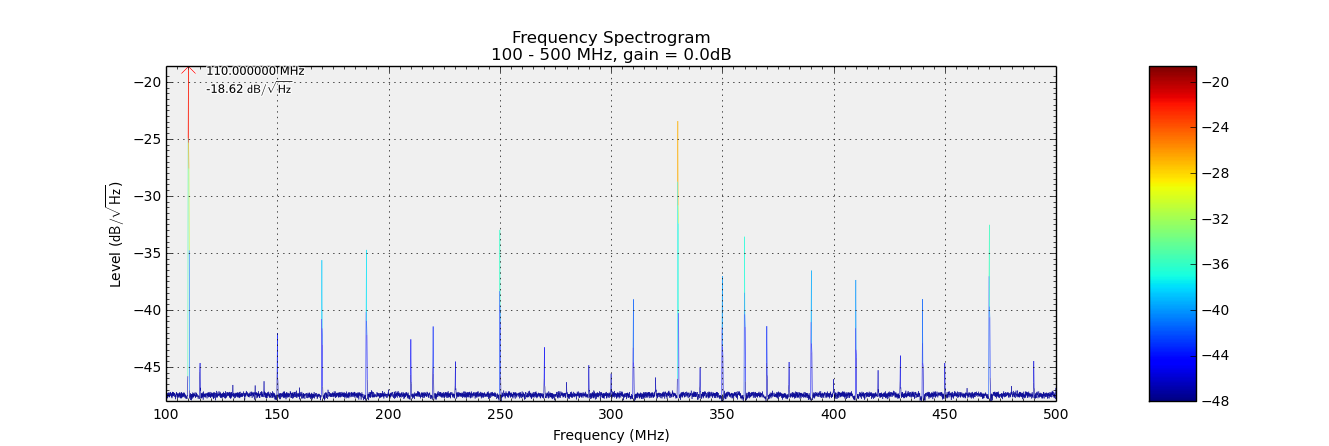
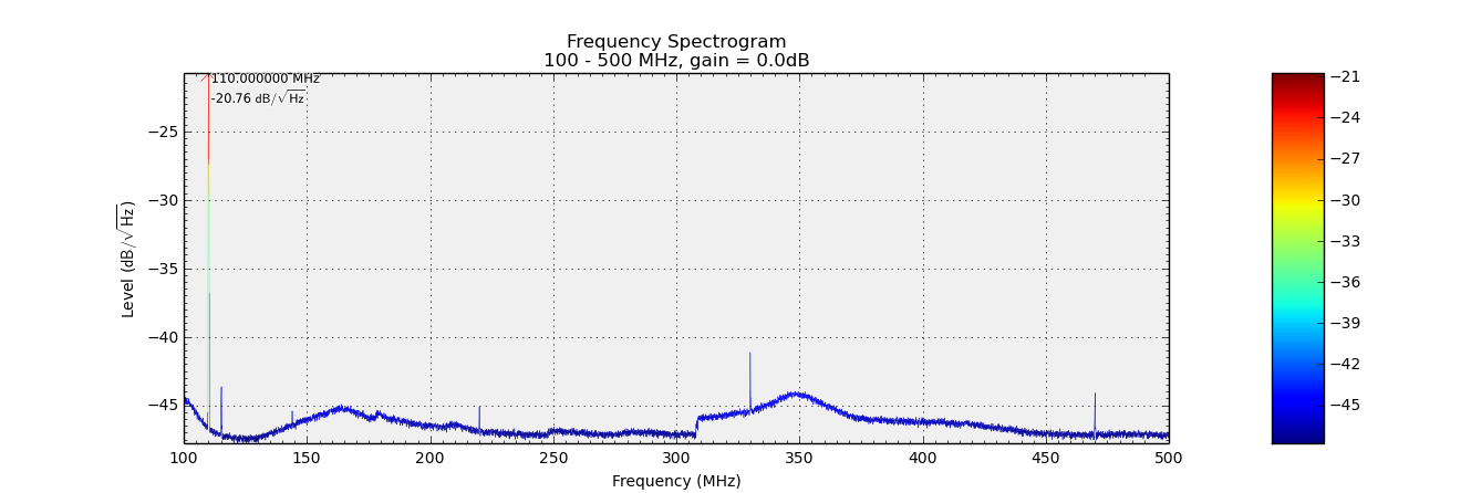
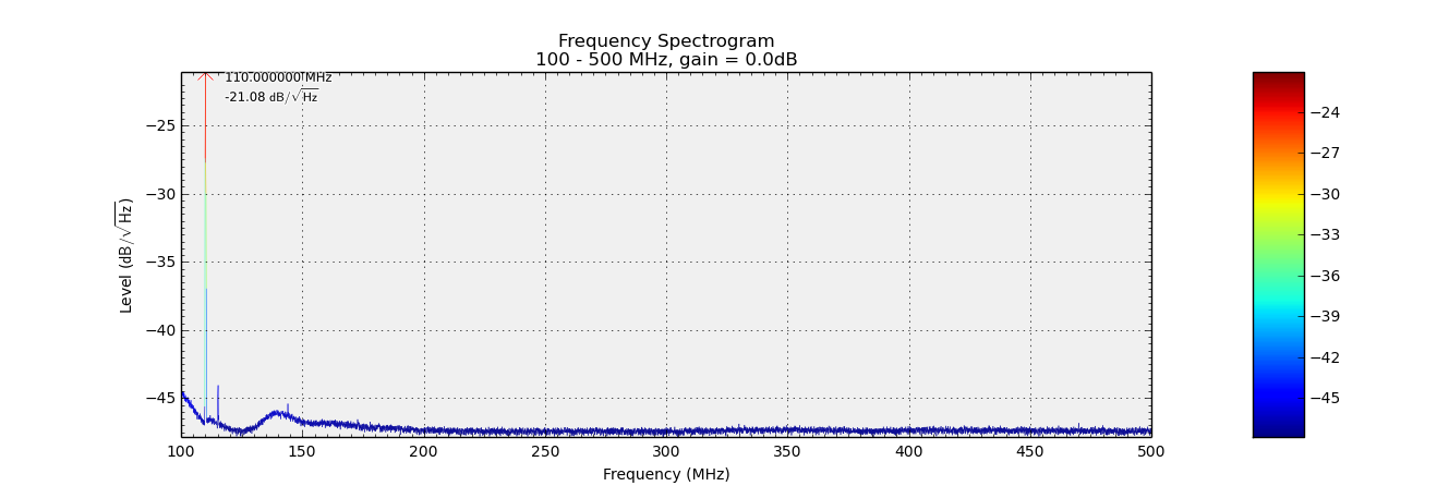
The effects of dithering can be seen in the following plots. In both plots, the
fundamental frequency is set to 110 MHz. With no dithering, there are many spurious
and harmonic emissions, with the largest being the third harmonic at 330 MHz.
With dithering applied, the strength of the third harmonic is greatly reduced,
and there are fewer spurious emissions. The power contained in the harmonics
has been spread evenly across the spectrum.
In the third plot a low pass filter has been added.
The second function is to serialise the 8 parallel data streams into a single stream of data before outputting on a logic pin. This is achieved using an OSERDES component.
A combination of dithering and filtering removes as much of the harmonic and spurious content as possible while still allowing a wide operating frequency range.
It is recommended that an additional band-pass filter (covering the band of operation) also be added between the transmitter and the antenna.
The Controller
The controller is written in C, and translated into Verilog using the Chips Compiler. The Controller provides a simple slave interface to drive the transmitter. A simple protocol allows the software running on the host to control the frequency, and the amplitude of the I and Q signal components. While the frequency can be updated at an arbitrary rate (controlled by a counter in the controller), the sample rate of the amplitude is determined by the sample frequency and the ratio of the interpolator and is fixed at 12KHz. The controller is also responsible for setting the frequency sample rate, and fetching a calibration value from the GPS hardware.
By allowing the host software direct control of the frequency and amplitude, all the commonly used analogue modes can be generated in the host software. FM modes require more bandwidth.
UART
The supported development cards all make use of the FTDI 2232H USB UART. The transmitter communicates to the FTDI chip using a light-weight UART. The UART is configured to run at the maximum rate supported by the USB chip of 12Mbit/s.
This allows some performance margin in Stereo FM which requires the most bandwidth of all the modes currently implemented. In stereo FM mode, the sample rate is 152 KHz, with a resolution of 16 bits. This requires a minimum transfer rate of 2.4Mbits/s
Within the receive half of the UART, an 8192 deep FIFO is employed. This provides sufficient buffering to allow smooth transmission of samples even when they are generated in software in real time.
GPS
The GPS interface consists of a second UART, which allows communication with the GPS module. The UART is not currently used, but could be used to decode NMEA messages from the GPS module.
The GPS interface also provides a counter running at 100MHz, which measures the length of the 1pps reference signal from the GPS module. The count value is used by the host software to measure the true frequency of the clock, and to make adjustments to the commanded frequency to compensate for any inaccuracies.
Software
The software is written in Python. The SciPy software stack consisting of NumPy, SciPy and Matplotlib is used for signal processing tasks. pySerial is used to interface to the hardware. wxPython provides the GUI framework. The SoX utility provides a portable interface to the audio system.
Initially, I thought that I might have to code some of the modulation schemes in C to get the necessary speed to run in real time. It turns out that the SciPy library provides acceptable real-time performance with no need for additional optimisations.
All the modulation techniques follow the same basic layout.
The input audio stream is converted to a floating point representation n the range -1 to + 1.
The audio is then low-pass filtered to suppress frequency components outside the band. They are then re-sampled to a working sample frequency. AM, FM and SSB modes use 12KHz, Wideband FM and Stereo FM use 48KHz to allow for the higher frequency content.
The data is then modulated and clipped, before being converted back to fixed point format. 16 bits (8 for I and 8 for Q) are used for IQ samples, and 16bits are used for frequency samples. The frequency samples are the fed to the transmitter hardware via the USB interface.
AM
AM is the simplest modulation scheme to implement. Audio samples are re-sampled to 12KHz, a DC offset is applied, and the data is duplicated in both I and Q channels.
SSB
In order to generate single sideband modulation, audio samples need to be converted into a complex representation containing only positive frequencies for upper sideband, and negative frequencies for lower sideband.
This is achieved by using an FIR filter to approximation of a Hilbert transform. The Hilbert transform shifts positive frequencies by 90 degrees, and negative frequencies by -90 degrees. When the transformed signal is added to the original transform, either the positive or negative frequencies cancel. A MATLAB Tutorial gives a straightforward introduction to the technique.

FM
Narrow band FM modulation is another very simple modulation scheme. The audio sample is multiplied by a constant to create a frequency sample with the required deviation.
WBFM
Wideband FM is similar to FM modulation, but used a larger constant to give the increased frequency deviation. In addition, the audio is first passed through pre-emphasis filter to boost higher frequency components.
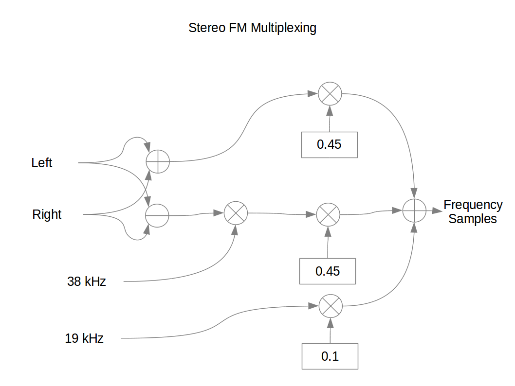
Stereo FM
In Stereo FM, sum and difference channel are formed by adding and subtracting the left and right channels. The sum channel is FM modulated in the normal way. The difference channel mixed with a 38KHz sub-carrier and added to sum channel. A 19KHz pilot tone (which is phase locked to the 38KHz sub-carrier) is also added to the sum channel. Since the stereo sub carrier adds inedible higher frequency components to the signal, a sample rate of 152KHz is used for the multiplexed stereo signal.
Further Work
There's plenty of potential for future development here. A few Ideas I would like to explore:
-
Add an FPGA based receive capability, perhaps by combining the ADCs built into the FPGA (1MS/s sampling rate 10 bits) with an external mixer, using the FPGA to provide a local oscillator.
-
Add CTCSS/DTS capability.
-
Explore cheaper hardware options such as iCEstick FPGA platform.