stffrdhrn / Sdram Controller
Labels
Projects that are alternatives of or similar to Sdram Controller
SDRAM Memory Controller
CURRENT STATUS : stable
This is a very a simple sdram controller which works on the De0 Nano. The project also contains a simple push button interface for testing on the dev board.
Basic features
- Operates at 100Mhz, CAS 3, 32MB, 16-bit data
- On reset will go into
INITsequnce - After
INITthe controller sits inIDLEwaiting forREFRESH,READorWRITE -
REFRESHoperations are spaced evenly 8192 times every 32ms -
READis always single read with auto precharge -
WRITEis always single write with auto precharge
 Host Interface          SDRAM Interface

   /-----------------------------\
   |      sdram_controller       |
==> wr_addr                  addr ==>
==> wr_data             bank_addr ==>
--> wr_enable                data <=>
   |                 clock_enable -->
==> rd_addr                  cs_n -->
--> rd_enable               ras_n -->
<== rd_data                 cas_n -->
<-- rd_ready                 we_n -->
<-- busy            data_mask_low -->
   |               data_mask_high -->
--> rst_n                        |
--> clk                          |
   \-----------------------------/
From the above diagram most signals should be pretty much self explainatory. Here are some important points for now. It will be expanded on later.
-
wr_addrandrd_addrare equivelant to the concatenation of{bank, row, column} -
rd_enableshould be set to high once an address is presented on theaddrbus and we wish to read data. -
wr_enableshould be set to high onceaddranddatais presented on the bus -
busywill go high when the read or write command is acknowledged.busywill go low when the write or read operation is complete. -
rd_readywill go high when datard_datais available on thedatabus. -
NOTE For single reads and writes
wr_enableandrd_enableshould be set low oncebusyis observed. This will protect from the controller thinking another request is needed if left higher any longer.
Build
The recommended way to build is to use fusesoc. The build steps are then:
# Build the project with quartus
fusesoc build dram_controller
# Program the project to de0 nano
fusesoc pgm dram_controller

# Build with icarus verilog and test
fusesoc sim dram_controller --vcd
gtkwave $fusebuild/dram_controller/sim-icarus/testlog.vcd

# Run other test cases
fusesoc sim --testbench fifo_tb dram_controller --vcd
fusesoc sim --testbench double_click_tb dram_controller --vcd
Timings
Initialization
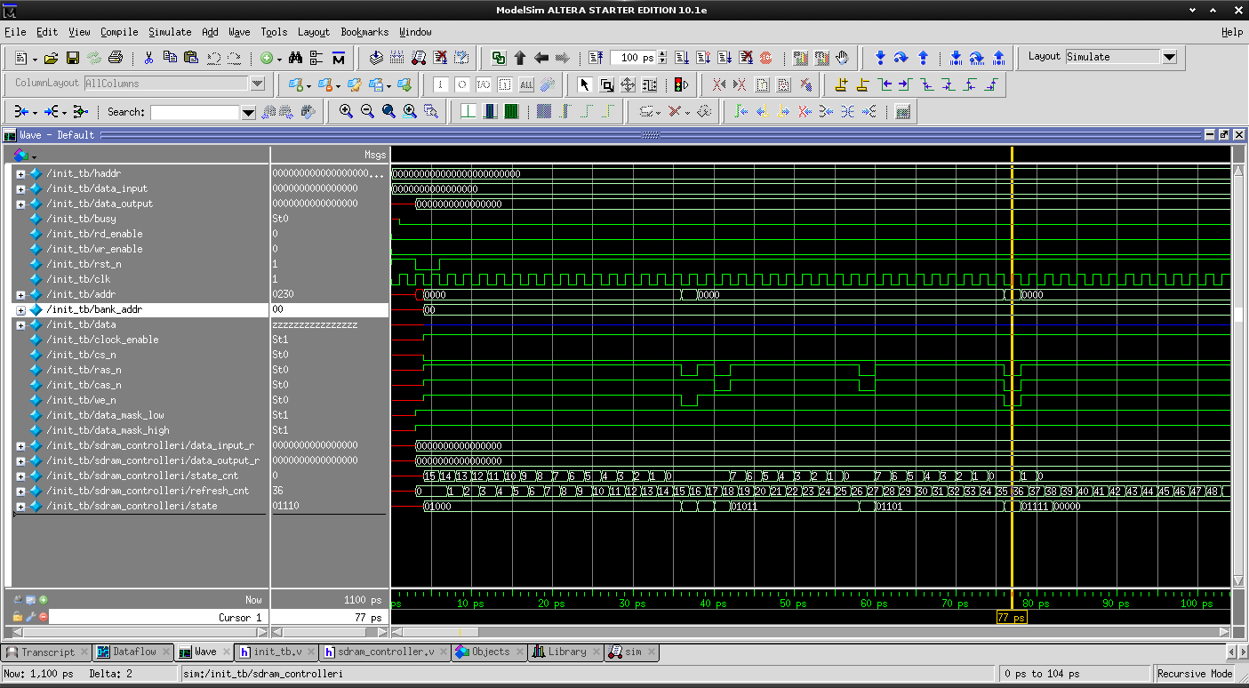
Initialization process showing:
- Precharge all banks
- 2 refresh cycles
- Mode programming
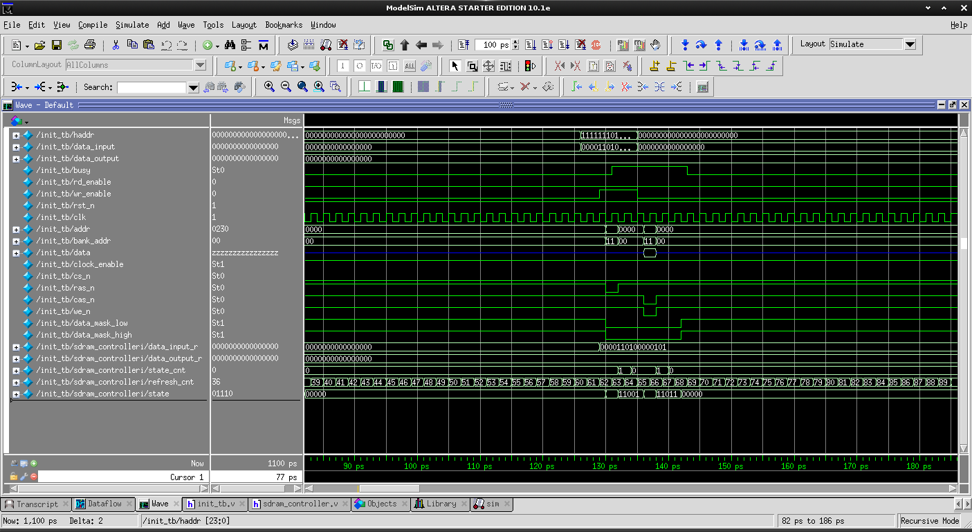
Refresh
Refresh process showing:
- Precharge all banks
- Single Refresh
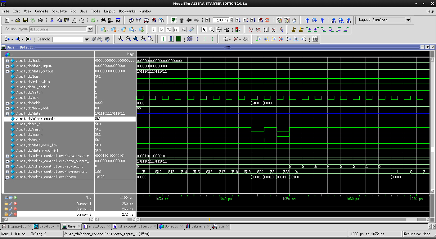
Writes
Write operation showing:
- Bank Activation & Row Address Strobe
- Column Address Strobe with Auto Precharge set and Data on bus
Reads
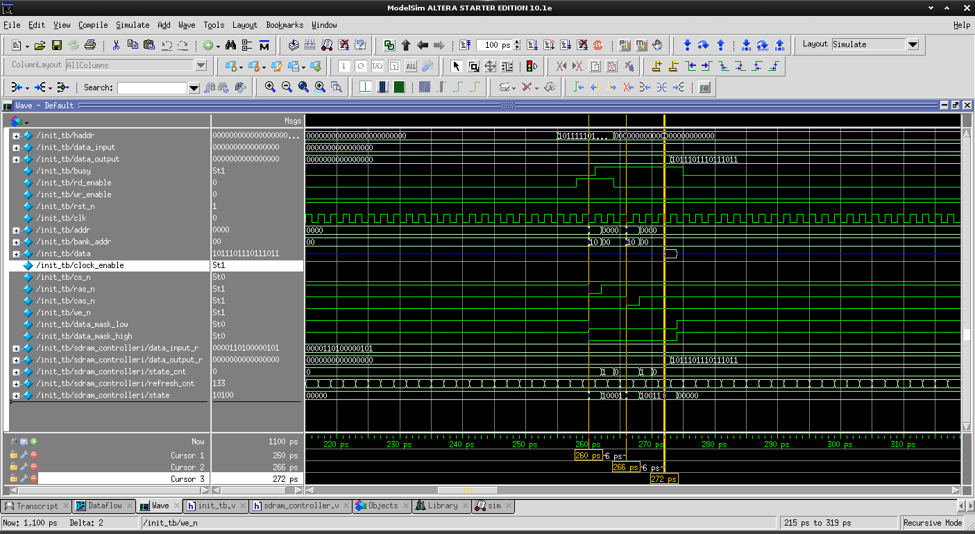
Read operation showing:
- Bank Activation & Row Address Strobe
- Column Address Strobe with Auto Precharge set
- Data on bus
Test Application
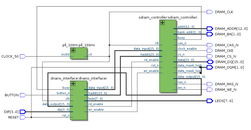 Figure - test application block diagram
The test application provides a simple user interface for testing the functionality of the sdram controller.
Basics:
- The clock input should be 50Mhz (a pll multiplies it up to 100Mhz)
- One push button is used for
reset - A Second push button is used for
readandwrite- single click for
write - double click for
read
- single click for
- A 4-bit dip switch is used for inputting addresses and data
- Upon
resetthe read/write addresses are read from the dip switch - When
writingthe dip switch is data is written to the sdram - Address and data busses are greather than 4 bits, data is duplicated to fill the bus
- Upon
- 8 LEDs are used to display the data read from the sdram. The data but is 16-bits, high and low bytes are alternated on the LEDs about every half second.
Project Status/TODO
- [x] Compiles
- [x] Simulated
Init - [x] Simulated
Refresh - [x] Simulated
Read - [x] Simulated
Write - [x] Confirmed in De0 Nano
Project Setup
This project has been developed with altera quartus II.
License
BSD
Further Reading
I didn't look at these when designing my controller. But it might be good to take a look at for ideas.
- http://hamsterworks.co.nz/mediawiki/index.php/Simple_SDRAM_Controller - featured on hackaday
- http://ladybug.xs4all.nl/arlet/fpga/source/sdram.v - Arlet's implementation from a comment on the hackaday article