stnolting / Neorv32
Projects that are alternatives of or similar to Neorv32
![]()
The NEORV32 RISC-V Processor
![]()
![]()


- Overview
- Status
- Features
- FPGA Implementation Results
- Performance
- Top Entities
- Getting Started
- Contribute/Feedback/Questions
- Legal
Overview
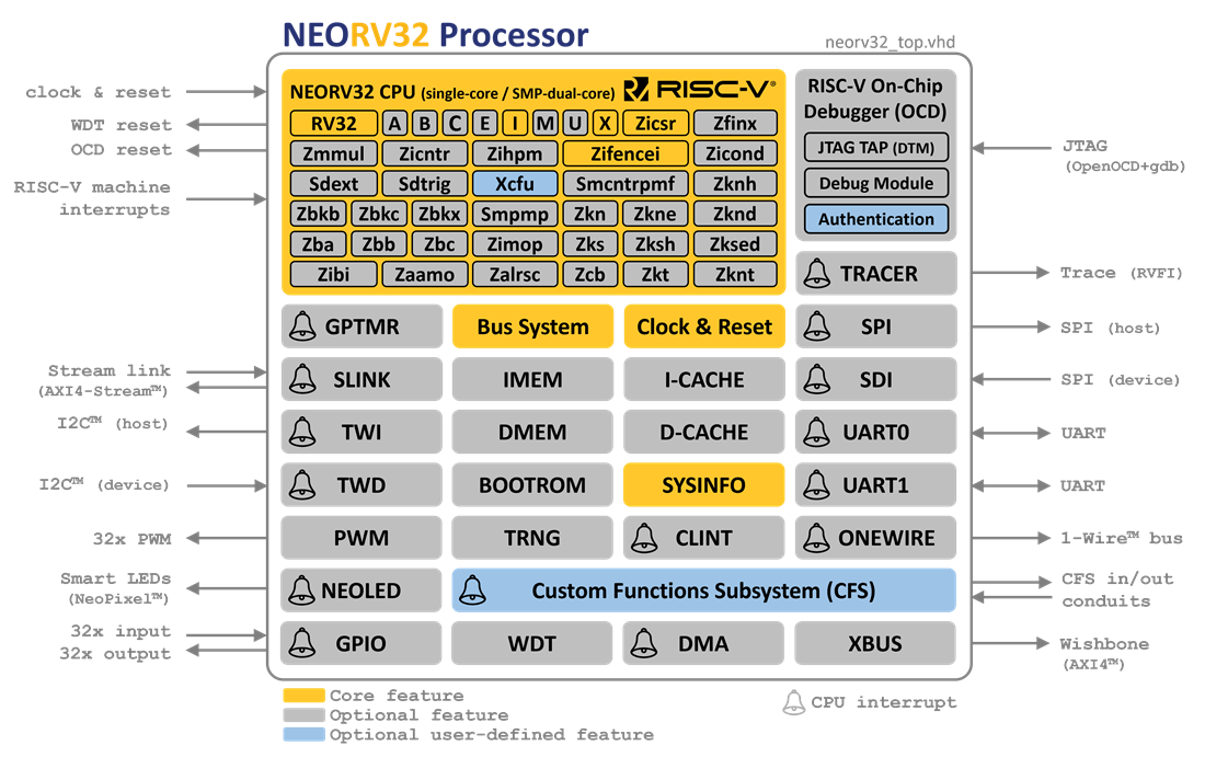
The NEORV32 Processor is a customizable microcontroller-like system on chip (SoC) that is based on the RISC-V NEORV32 CPU. The processor is intended as ready-to-go auxiliary processor within a larger SoC designs or as stand-alone custom microcontroller.
📚 For detailed information take a look at the NEORV32 data sheet (pdf). The doxygen-based documentation of the software framework is available online at GitHub-pages.
🏷 The project’s change log is available as CHANGELOG.md in the root directory of this repository. To see the changes between stable releases visit the project's release page.
🗒 Check out the project boards for a list of current ideas, TODOs, features being planned and work-in-progress.
💡 Feel free to open a new issue or start a new discussion if you have questions, comments, ideas or bug-fixes. Check out how to contribute.
Key Features
- RISC-V 32-bit
rv32NEORV32 CPU, compatible to- subset of the Unprivileged ISA Specification (Version 2.2)
- subset of the Privileged Architecture Specification (Version 1.12-draft)
- the official RISC-V architecture tests (passing)
- Configurable RISC-V-compatible CPU extensions
-
A- atomic memory access instructions (optional) -
B- Bit manipulation instructions (optional) 🚧 -
C- compressed instructions (16-bit) (optional) -
E- embedded CPU (reduced register file size) (optional) -
I- base integer instruction set (always enabled) -
M- integer multiplication and division hardware (optional) -
U- less-privileged user mode (optional) -
X- NEORV32-specific extensions (always enabled) -
Zicsr- control and status register access instructions (+ exception/irq system) (optional) -
Zifencei- instruction stream synchronization (optional) -
PMP- physical memory protection (optional) -
HPM- hardware performance monitors (optional)
-
- Full-scale RISC-V microcontroller system / SoC NEORV32 Processor with optional submodules
- optional embedded memories (instructions/data/bootloader, RAM/ROM) and caches
- timers (watch dog, RISC-V-compatible machine timer)
- serial interfaces (SPI, TWI, UARTs)
- general purpose IO and PWM channels
- external bus interface (Wishbone / AXI4)
- dedicated NeoPixel(TM) LED interface
- subsystem for custom co-processors
- more ...
- Software framework
- core libraries for high-level usage of the provided functions and peripherals
- application compilation based on GNU makefiles
- GCC-based toolchain (pre-compiled toolchains available)
- bootloader with UART interface console
- runtime environment
- several example programs
- doxygen-based software documentation: available on GitHub pages
- FreeRTOS port available
- Full-blown data sheet (pdf)
- Completely described in behavioral, platform-independent VHDL - no primitives, macros, etc.
- Fully synchronous design, no latches, no gated clocks
- Small hardware footprint and high operating frequency
Design Principles
- From zero to hello_world: Completely open source and documented.
- Plain VHDL without technology-specific parts like attributes, macros or primitives.
- Easy to use – working out of the box.
- Clean synchronous design, no wacky combinatorial interfaces.
- Be as small as possible – but with a reasonable size-performance trade-off.
- Be as RISC-V-compliant as possible.
- The processor has to fit in a Lattice iCE40 UltraPlus 5k low-power FPGA running at 22+ MHz.
Status
The processor is synthesizable (tested on real hardware using Intel Quartus Prime, Xilinx Vivado and Lattice Radiant/Synplify Pro) and can successfully execute all the provided example programs including the CoreMark benchmark.
RISC-V Architecture Tests: The processor passes the official rv32_m/C, rv32_m/I, rv32_m/M, rv32_m/privilege and rv32_m/Zifencei
riscv-arch-test tests. More information regarding the NEORV32 port of the riscv-arch-test test framework can be found in
riscv-arch-test/README.md.
| Project component | CI status |
|---|---|
| NEORV32 processor | |
| SW Framework Documentation (online at GH-pages) | |
| Pre-built toolchains | |
| RISC-V architecture test |
Features
The full-blown data sheet of the NEORV32 Processor and CPU is available as pdf file: 📄 NEORV32 data sheet.
NEORV32 Processor Features
The NEORV32 Processor provides a full-scale microcontroller-like SoC based on the NEORV32 CPU. The setup is highly customizable via the processor's top generics and already provides the following optional modules:
- processor-internal data and instruction memories (DMEM / IMEM) & cache (iCACHE)
- bootloader (BOOTLDROM) with UART console and automatic application boot from SPI flash option
- machine system timer (MTIME), RISC-V-compatible
- watchdog timer (WDT)
- two independent universal asynchronous receivers and transmitters (UART0 & UART1) with optional hardware flow control (RTS/CTS)
- 8/16/24/32-bit serial peripheral interface controller (SPI) with 8 dedicated chip select lines
- two wire serial interface controller (TWI), with optional clock-stretching, compatible to the I²C standard
- general purpose parallel IO port (GPIO), 32xOut & 32xIn, with pin-change interrupt
- 32-bit external bus interface, Wishbone b4 compatible (WISHBONE)
- wrapper for AXI4-Lite Master Interface (see AXI Connectivity)
- PWM controller with 4 channels and 8-bit duty cycle resolution (PWM)
- ring-oscillator-based true random number generator (TRNG)
- custom functions subsystem (CFS) for tightly-coupled custom co-processor extensions
- numerically-controlled oscillator (NCO) with three independent channels
- smart LED interface (NEOLED) - WS2812 / NeoPixel(c) compatible
- system configuration information memory to check hardware configuration by software (SYSINFO)
NEORV32 CPU Features
The NEORV32 CPU implements the official RISC-V specifications (2.2) including a subset of the RISC-V privileged architecture specifications (1.12-draft)
- tested via the official riscv-arch-test Test Framework
(see
riscv-arch-test/README).
More information regarding the CPU including a detailed list of the instruction set and the available CSRs can be found in the 📄 NEORV32 data sheet.
General Features
- Modified Harvard architecture (separate CPU interfaces for data and instructions; NEORV32 processor: Single processor-internal bus via I/D mux)
- Two stages in-order pipeline (FETCH, EXECUTE); each stage uses a multi-cycle processing scheme
- No hardware support of unaligned accesses - they will trigger an exception
- BIG-ENDIAN byte-order, processor's external memory interface allows endianness configuration to connect to system with different endianness
- All reserved or unimplemented instructions will raise an illegal instruction exception
- Privilege levels:
machinemode,usermode (if enabled viaUextension) - Official RISC-V open-source architecture ID
A - Atomic memory access extension
- Supported instructions:
LR.W(load-reservate)SC.W(store-conditional)
B - Bit manipulation instructions extension
- 🚧 work-in-progress 🚧
- ⚠️ this extension has not been officially ratified yet!
- 📚 more information can be found here: RISC-V
Bspec. - Compatible to v0.94-draft of the bit manipulation spec
- Support via intrinsic library (see
sw/example/bit_manipulation) -
Zbbbase instruction set:CLZCTZCPOPSEXT.BSEXT.HMIN[U]MAX[U]ANDNORNXNORROLROR[I]zext(pseudo-instruction forPACK rd, rs, zero)rev8(pseudo-instruction forGREVI rd, rs, -8)orc.b(pseudo-instruction forGORCI rd, rs, 7) -
Zbssingle-bit instructions:SBSET[I]SBCLR[I]SBINV[I]SBEXT[I] -
Zbashifted-add instructions:SH1ADDSH2ADDSH3ADD
C - Compressed instructions extension
- ALU instructions:
C.ADDI4SPNC.ADD[I]C.ADDI16SPC.LIC.LUIC.SLLIC.SRLIC.SRAIC.ANDIC.SUBC.XORC.ORC.ANDC.MVC.NOP - Jump and branch instructions:
C.JC.JALC.JRC.JALRC.BEQZC.BNEZ - Memory instructions:
C.LWC.SWC.LWSPC.SWSP - System instructions:
C.EBREAK(requiresZicsrextension) - Pseudo-instructions are not listed
E - Embedded CPU version extension
- Reduced register file (only the 16 lowest registers are implemented)
I - Base integer instruction set
- ALU instructions:
LUIAUIPCADD[I]SLT[I][U]XOR[I]OR[I]AND[I]SLL[I]SRL[I]SRA[I]SUB - Jump and branch instructions:
JALJALRBEQBNEBLTBGEBLTUBGEU - Memory instructions:
LBLHLWLBULHUSBSHSW - System instructions:
ECALLEBREAKFENCE - Pseudo-instructions are not listed
M - Integer multiplication and division hardware extension
- Multiplication instructions:
MULMULHMULHSUMULHU - Division instructions:
DIVDIVUREMREMU - By default, the multiplier and divider cores use an iterative bit-serial processing scheme
- Multiplications can be mapped to DSPs via the
FAST_MUL_ENgeneric to increase performance
U - Privileged architecture - User mode extension
- Requires
Zicsrextension - Privilege levels:
M(machine mode) + less-privilegedU(user mode)
X - NEORV32-specific CPU extensions
- The NEORV32-specific extensions are always enabled and are indicated via the
Xbit set in themisaCSR. - 16 fast interrupt request channels with according control/status bits in
mieandmipand custom exception codes inmcause -
mzextCSR to check for implementedZ*CPU extensions (likeZifencei) - All undefined/umimplemented/malformed/illegal instructions do raise an illegal instruction exception
Zfinx - Single-precision floating-point extension (using integer x registers)
- 🚧 work-in-progress 🚧
- ⚠️ this extension has not been officially ratified yet!
- 📚 more information can be found here: RISC-V
Zfinxspec. - ℹ️ check out the floating-point extension project board for the current implementation state
Zicsr - Privileged architecture - CSR access extension
- Privilege levels:
M-mode(Machine mode) - CSR access instructions:
CSRRW[I]CSRRS[I]CSRRC[I] - System instructions:
MRETWFI - Pseudo-instructions are not listed
- Counter CSRs:
[m]cycle[h][m]instret[m]time[h][m]hpmcounter*[h](3..31, configurable)mcounterenmcountinhibitmhpmevent*(3..31, configurable) - Machine CSRs:
mstatus[h]misa(read-only!)miemtvecmscratchmepcmcausemtvalmipmvendoridmarchidmimpidmhartidmzext(custom) - Supported (sync.) exceptions (implementing the RISC-V specs):
- Misaligned instruction address
- Instruction access fault (via timeout/error after unacknowledged bus access)
- Illegal instruction
- Breakpoint (via
ebreakinstruction) - Load address misaligned
- Load access fault (via timeout/error after unacknowledged bus access)
- Store address misaligned
- Store access fault (via unacknowledged bus access after timeout)
- Environment call from U-mode (via
ecallinstruction in user mode) - Environment call from M-mode (via
ecallinstruction in machine mode)
- Supported (async.) exceptions / interrupts:
- Machine timer interrupt
mti(via processor's MTIME unit / external signal) - Machine software interrupt
msi(via external signal) - Machine external interrupt
mei(via external signal) - 16 fast interrupt requests (custom extension), 6+1 available for custom usage
- Machine timer interrupt
Zifencei - Privileged architecture - Instruction stream synchronization extension
- System instructions:
FENCE.I(among others, used to clear and reload instruction cache)
PMP - Privileged architecture - Physical memory protection
- Requires
Zicsrextension - Configurable number of regions (0..63)
- Additional machine CSRs:
pmpcfg*(0..15)pmpaddr*(0..63)
HPM - Privileged architecture - Hardware performance monitors
- Requires
Zicsrextension - Configurable number of counters (0..29)
- Additional machine CSRs:
mhpmevent*(3..31)[m]hpmcounter*[h](3..31)
⚠️ Non-RISC-V-Compatible Issues and Limitations
- CPU and Processor are BIG-ENDIAN, but this should be no problem as the external memory bus interface provides big- and little-endian configurations
-
misaCSR is read-only - no dynamic enabling/disabling of synthesized CPU extensions during runtime; for compatibility: write accesses (in m-mode) are ignored and do not cause an exception - The physical memory protection (PMP) only supports
NAPOTmode yet and a minimal granularity of 8 bytes - The
Aextension only implementslr.wandsc.winstructions yet. However, these instructions are sufficient to emulate all further AMO operations - The
mcausetrap code0x80000000(originally reserved in the RISC-V specs) is used to indicate a hardware reset (as "non-maskable interrupt") - The bit manipulation extension is not yet officially ratified, but is expected to stay unchanged. There is no software support in the upstream GCC RISC-V port yet. However, an intrinsic library is provided to utilize the provided bit manipulation extension from C-language code (see
sw/example/bit_manipulation). NEORV32'sBextension is compatible to spec. version "0.94-draft".
FPGA Implementation Results
NEORV32 CPU
This chapter shows exemplary implementation results of the NEORV32 CPU for an Intel Cyclone IV EP4CE22F17C6N FPGA on a DE0-nano board. The design was synthesized using Intel Quartus Prime Lite 20.1 ("balanced implementation"). The timing information is derived from the Timing Analyzer / Slow 1200mV 0C Model. If not otherwise specified, the default configuration of the CPU's generics is assumed (e.g. no physical memory protection, no hardware performance monitors). No constraints were used at all.
Results generated for hardware version 1.5.1.4.
| CPU Configuration | LEs | FFs | Memory bits | DSPs | f_max |
|---|---|---|---|---|---|
rv32i |
979 | 409 | 1024 | 0 | 123 MHz |
rv32i + Zicsr
|
1789 | 847 | 1024 | 0 | 122 MHz |
rv32im + Zicsr
|
2381 | 1125 | 1024 | 0 | 122 MHz |
rv32imc + Zicsr
|
2608 | 1140 | 1024 | 0 | 122 MHz |
rv32imac + Zicsr
|
2621 | 1144 | 1024 | 0 | 122 MHz |
rv32imacb + Zicsr
|
3013 | 1310 | 1024 | 0 | 122 MHz |
rv32imacb + Zicsr + u
|
3031 | 1313 | 1024 | 0 | 122 MHz |
rv32imacb + Zicsr + u + Zifencei
|
3050 | 1313 | 1024 | 0 | 116 MHz |
Setups with enabled "embedded CPU extension" E show the same LUT and FF utilization and identical f_max as the according I configuration.
However, the size of the register file is cut in half.
NEORV32 Processor-Internal Peripherals and Memories
Results generated for hardware version 1.5.2.4.
| Module | Description | LEs | FFs | Memory bits | DSPs |
|---|---|---|---|---|---|
| BOOT ROM | Bootloader ROM (default 4kB) | 3 | 1 | 32 768 | 0 |
| BUSSWITCH | Bus mux for CPU instr. & data interfaces | 65 | 8 | 0 | 0 |
| i-CACHE | Proc.-int. nstruction cache (default 1x4x64 bytes) | 234 | 156 | 8 192 | 0 |
| CFS | Custom functions subsystem | - | - | - | - |
| DMEM | Processor-internal data memory (default 8kB) | 6 | 2 | 65 536 | 0 |
| GPIO | General purpose input/output ports | 67 | 65 | 0 | 0 |
| IMEM | Processor-internal instruction memory (default 16kb) | 6 | 2 | 131 072 | 0 |
| MTIME | Machine system timer | 274 | 166 | 0 | 0 |
| NCO | Numerically-controlled oscillator | 254 | 226 | 0 | 0 |
| NEOLED | Smart LED Interface (NeoPixel-compatibile) [4x FIFO] | 347 | 309 | 0 | 0 |
| PWM | Pulse-width modulation controller | 71 | 69 | 0 | 0 |
| SPI | Serial peripheral interface | 138 | 124 | 0 | 0 |
| SYSINFO | System configuration information memory | 11 | 10 | 0 | 0 |
| TRNG | True random number generator | 132 | 105 | 0 | 0 |
| TWI | Two-wire interface | 77 | 46 | 0 | 0 |
| UART0/1 | Universal asynchronous receiver/transmitter 0/1 | 176 | 132 | 0 | 0 |
| WDT | Watchdog timer | 60 | 45 | 0 | 0 |
| WISHBONE | External memory interface | 129 | 104 | 0 | 0 |
NEORV32 Processor - Exemplary FPGA Setups
Exemplary processor implementation results for different FPGA platforms. The processor setup uses the default peripheral configuration (like no CFS and no TRNG), no external memory interface and only internal instruction and data memories. IMEM uses 16kB and DMEM uses 8kB memory space. The setup's top entity connects most of the processor's top entity signals to FPGA pins - except for the Wishbone bus and the interrupt signals. The "default" strategy of each toolchain is used.
Results generated for hardware version 1.4.9.0.
| Vendor | FPGA | Board | Toolchain | CPU Configuration | LUT / LE | FF / REG | DSP | Memory Bits | BRAM / EBR | SPRAM | Frequency |
|---|---|---|---|---|---|---|---|---|---|---|---|
| Intel | Cyclone IV EP4CE22F17C6N
|
Terasic DE0-Nano | Quartus Prime Lite 20.1 |
rv32imc + u + Zicsr + Zifencei
|
3813 (17%) | 1904 (8%) | 0 (0%) | 231424 (38%) | - | - | 119 MHz |
| Lattice | iCE40 UltraPlus iCE40UP5K-SG48I
|
Upduino v2.0 | Radiant 2.1 (Synplify Pro) |
rv32ic + u + Zicsr + Zifencei
|
4397 (83%) | 1679 (31%) | 0 (0%) | - | 12 (40%) | 4 (100%) | c 22.15 MHz |
| Xilinx | Artix-7 XC7A35TICSG324-1L
|
Arty A7-35T | Vivado 2019.2 |
rv32imc + u + Zicsr + Zifencei + PMP
|
2465 (12%) | 1912 (5%) | 0 (0%) | - | 8 (16%) | - | c 100 MHz |
Notes
- The Lattice iCE40 UltraPlus setup uses the FPGA's SPRAM memory primitives for the internal IMEM and DMEM (each 64kb).
The FPGA-specific memory components can be found in
rtl/fpga_specific. - The clock frequencies marked with a "c" are constrained clocks. The remaining ones are f_max results from the place and route timing reports.
- The Upduino and the Arty board have on-board SPI flash memories for storing the FPGA configuration. These device can also be used by the default NEORV32 bootloader to store and automatically boot an application program after reset (both tested successfully).
- The setups with
PMPimplement 2 regions with a minimal granularity of 64kB. - No HPM counters are implemented.
Performance
CoreMark Benchmark
The CoreMark CPU benchmark was executed on the NEORV32 and is available in the sw/example/coremark project folder. This benchmark tests the capabilities of a CPU itself rather than the functions provided by the whole system / SoC.
**Configuration**
Hardware:       32kB IMEM, 16kB DMEM, no caches, 100MHz clock
CoreMark:       2000 iterations, MEM_METHOD is MEM_STACK
Compiler:       RISCV32-GCC 10.1.0 (rv32i toolchain)
Compiler flags: default, see makefile
Peripherals:    UART for printing the results
Results generated for hardware version 1.4.9.8.
CPU (including Zicsr) |
Executable Size | Optimization | CoreMark Score | CoreMarks/MHz |
|---|---|---|---|---|
rv32i |
28 756 bytes | -O3 |
36.36 | 0.3636 |
rv32im |
27 516 bytes | -O3 |
68.97 | 0.6897 |
rv32imc |
22 008 bytes | -O3 |
68.97 | 0.6897 |
rv32imc + FAST_MUL_EN
|
22 008 bytes | -O3 |
86.96 | 0.8696 |
rv32imc + FAST_MUL_EN + FAST_SHIFT_EN
|
22 008 bytes | -O3 |
90.91 | 0.9091 |
The FAST_MUL_EN configuration uses DSPs for the multiplier of the M extension (enabled via the FAST_MUL_EN generic). The FAST_SHIFT_EN configuration
uses a barrel shifter for CPU shift operations (enabled via the FAST_SHIFT_EN generic).
When the C extension is enabled, branches to an unaligned uncompressed instruction require additional instruction fetch cycles.
Instruction Cycles
The NEORV32 CPU is based on a two-stages pipelined architecutre. Each stage uses a multi-cycle processing scheme. Hence,
each instruction requires several clock cycles to execute (2 cycles for ALU operations, ..., 40 cycles for divisions).
The average CPI (cycles per instruction) depends on the instruction mix of a specific applications and also on the available
CPU extensions. By default the CPU-internal shifter (e.g. for the SLL instruction) as well as the multiplier and divider of the
M extension use a bit-serial approach and require several cycles for completion.
The following table shows the performance results for successfully running 2000 CoreMark
iterations, which reflects a pretty good "real-life" work load. The average CPI is computed by
dividing the total number of required clock cycles (only the timed core to avoid distortion due to IO wait cycles; sampled via the cycle[h] CSRs)
by the number of executed instructions (instret[h] CSRs). The executables were generated using optimization -O3.
Results generated for hardware version 1.4.9.8.
CPU (including Zicsr) |
Required Clock Cycles | Executed Instructions | Average CPI |
|---|---|---|---|
rv32i |
5 595 750 503 | 1 466 028 607 | 3.82 |
rv32im |
2 966 086 503 | 598 651 143 | 4.95 |
rv32imc |
2 981 786 734 | 611 814 918 | 4.87 |
rv32imc + FAST_MUL_EN
|
2 399 234 734 | 611 814 918 | 3.92 |
rv32imc + FAST_MUL_EN + FAST_SHIFT_EN
|
2 265 135 174 | 611 814 948 | 3.70 |
The FAST_MUL_EN configuration uses DSPs for the multiplier of the M extension (enabled via the FAST_MUL_EN generic). The FAST_SHIFT_EN configuration
uses a barrel shifter for CPU shift operations (enabled via the FAST_SHIFT_EN generic).
When the C extension is enabled branches to an unaligned uncompressed instruction require additional instruction fetch cycles.
Top Entities
The top entity of the NEORV32 Processor (SoC) is rtl/core/neorv32_top.vhd,
which provides a Wishbone b4-compatoible bus interface.
ℹ️ It is recommended to use the processor setup even if you want to use the CPU in stand-alone mode. Simply disable all the processor-internal modules via the generics and you will get a "CPU wrapper" that already provides a minimal CPU environment and an external memory interface (like AXI4). This setup also allows to further use the default bootloader and software framework. From this base you can start building your own processor system.
Use the top's generics to configure the system according to your needs. Each generic is initilized with the default configuration. Detailed information regarding the interface signals and configuration generics can be found in the 📄 NEORV32 data sheet (pdf).
All signals of the top entity are of type std_ulogic or std_ulogic_vector, respectively (except for the processor's TWI signals, which are of type std_logic). Leave all unused output ports unconnected and tie all unused input ports to zero.
Alternative top entities, like the simplified "hello world" test setup or CPU/Processor
wrappers with resolved port signal types (i.e. std_logic), can be found in rtl/top_templates.
AXI4 Connectivity
Via the rtl/top_templates/neorv32_top_axi4lite.vhd
wrapper the NEORV32 provides an AXI4-Lite compatible master interface. This wrapper instantiates the default
NEORV32 processor top entitiy and implements a Wishbone to AXI4-Lite bridge.
The AXI4-Lite interface has been tested using Xilinx Vivado 19.2 block designer:

The processor was packed as custom IP using neorv32_top_axi4lite.vhd as top entity. The AXI interface is automatically detected by the packager.
All remaining IO interfaces are available as custom signals. The configuration generics are available via the "customize IP" dialog.
In the figure above the resulting IP block is named "neorv32_top_axi4lite_v1_0".
(Note: Use Syntheiss option "global" when generating the block design to maintain the internal TWI tri-state drivers.)
The setup uses an AXI interconnect to attach two block RAMs to the processor. Since the processor in this example is configured without IMEM and DMEM,
the attached block RAMs are used for storing instructions and data: the first RAM is used as instruction memory
and is mapped to address 0x00000000 - 0x00003fff (16kB), the second RAM is used as data memory and is mapped to address 0x80000000 - 0x80001fff (8kB).
Getting Started
This overview is just a short excerpt from the Let's Get It Started section of the NEORV32 documentary:
1. Get the Toolchain
At first you need a RISC-V GCC toolchain. You can either download the sources and build the toolchain by yourself, or you can download a prebuilt one and install it.
To build the toolchain by yourself, follow the official build instructions.
Make sure to use the ilp32 or ilp32e ABI.
Alternatively, you can download a prebuilt toolchain. I have uploaded the toolchains I am using to GitHub. These toolchains were compiled on a 64-bit x86 Ubuntu 20.04 LTS (Ubuntu on Windows, actually). Download the toolchain of choice: github.com/stnolting/riscv-gcc-prebuilt
You can also use the toolchains provided by SiFive. These are 64-bit toolchains that can also emit 32-bit
RISC-V code. They were compiled for more sophisticated machines (rv32imac) so make sure the according NEORV32 hardware extensions are enabled.
⚠️ Keep in mind that – for instance – a rv32imc toolchain only provides library code compiled with compressed and
mul/div instructions! Hence, this code cannot be executed (without emulation) on an architecture without these extensions!
To check everything works fine, make sure GNU Make and a native GCC compiler are installed.
Test the installation of the RISC-V toolchain by navigating to an example program project like
sw/example/blink_led and running:
neorv32/sw/example/blink_led$ make check
2. Download the NEORV32 Project
Get the sources of the NEORV32 Processor project. The simplest way is using git clone (suggested for easy project updates via git pull):
$ git clone https://github.com/stnolting/neorv32.git
Alternatively, you can either download a specific release or get the most recent version
of this project as *.zip file.
3. Create a new FPGA Project
Create a new project with your FPGA design tool of choice. Add all the *.vhd files from the rtl/core
folder to this project. Make sure to add these files to a new design library called neorv32.
You can either instantiate the processor's top entity or one of its
wrappers in your own project. If you just want to try thing out,
you can use the simple test setup (rtl/top_templates/neorv32_test_setup.vhd) as top entity.
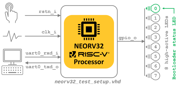
This test setup instantiates the processor and implements most of the peripherals and some ISA extensions. Only the UART0 communications lines, clock, reset and some GPIO output signals are propagated as actual top entity interface signals. Basically, it is a FPGA version of a "hello world" example:
  entity neorv32_test_setup is
    port (
      -- Global control --
      clk_i       : in  std_ulogic := '0'; -- global clock, rising edge
      rstn_i      : in  std_ulogic := '0'; -- global reset, low-active, async
      -- GPIO --
      gpio_o      : out std_ulogic_vector(7 downto 0); -- parallel output
      -- UART0 --
      uart0_txd_o : out std_ulogic;       -- UART0 send data
      uart0_rxd_i : in  std_ulogic := '0' -- UART0 receive data
    );
  end neorv32_test_setup;
4. Compile an Example Program
The NEORV32 project includes several example program project from which you can start your own application. There are example programs to check out the processor's peripheral like I2C or the true-random number generator. And yes, there is also a port of Conway's Game of Life available! 😉
Simply compile one of these projects using
neorv32/sw/example/blink_led$ make clean_all exe
This will create a NEORV32 executable neorv32_exe.bin in the same folder, which you can upload via the bootloader.
5. Upload the Executable via the Bootloader
Connect your FPGA board via UART to your computer and open the according port to interface with the fancy NEORV32 bootloader. The bootloader uses the following default UART configuration:
- 19200 Baud
- 8 data bits
- 1 stop bit
- No parity bits
- No transmission / flow control protocol (raw bytes only)
- Newline on
\r\n(carriage return & newline) - also for sent data
Use the bootloader console to upload the neorv32_exe.bin executable gerated during application compiling and run your application.
<< NEORV32 Bootloader >>

BLDV: Nov  7 2020
HWV:  0x01040606
CLK:  0x0134FD90 Hz
USER: 0x0001CE40
MISA: 0x42801104
PROC: 0x03FF0035
IMEM: 0x00010000 bytes @ 0x00000000
DMEM: 0x00010000 bytes @ 0x80000000

Autoboot in 8s. Press key to abort.
Aborted.

Available CMDs:
 h: Help
 r: Restart
 u: Upload
 s: Store to flash
 l: Load from flash
 e: Execute
CMD:> u
Awaiting neorv32_exe.bin... OK
CMD:> e
Booting...

Blinking LED demo program
Going further: Take a look at the Let's Get It Started! chapter of the 📄 NEORV32 data sheet.
Contribute/Feedback/Questions
I'm always thankful for help! So if you have any questions, bug reports, ideas or if you want to give any kind of feedback, feel free to open a new issue, start a new discussion on GitHub or directly drop me a line.
Here is a simple guide line if you'd like to contribute to this repository:
- ⭐️ this repository 😉
- Check out the project's code of conduct
- Fork this repository and clone the fork
- Create a feature branch in your fork:
git checkout -b awesome_new_feature_branch - Create a new remote for the upstream repo:
git remote add upstream https://github.com/stnolting/neorv32 - Commit your modifications:
git commit -m "Awesome new feature!" - Push to the branch:
git push origin awesome_new_feature_branch - Create a new pull request
Legal
This project is released under the BSD 3-Clause license. No copyright infringement intended. Other implied or used projects might have different licensing - see their documentation to get more information.
Citing
If you are using the NEORV32 or parts of the project in some kind of publication, please cite it as follows:
S. Nolting, "The NEORV32 RISC-V Processor", github.com/stnolting/neorv32
BSD 3-Clause License
Copyright (c) 2021, Stephan Nolting. All rights reserved.
Redistribution and use in source and binary forms, with or without modification, are permitted provided that the following conditions are met:
- Redistributions of source code must retain the above copyright notice, this list of conditions and the following disclaimer.
- Redistributions in binary form must reproduce the above copyright notice, this list of conditions and the following disclaimer in the documentation and/or other materials provided with the distribution.
- Neither the name of the copyright holder nor the names of its contributors may be used to endorse or promote products derived from this software without specific prior written permission.
THIS SOFTWARE IS PROVIDED BY THE COPYRIGHT HOLDERS AND CONTRIBUTORS "AS IS" AND ANY EXPRESS OR IMPLIED WARRANTIES, INCLUDING, BUT NOT LIMITED TO, THE IMPLIED WARRANTIES OF MERCHANTABILITY AND FITNESS FOR A PARTICULAR PURPOSE ARE DISCLAIMED. IN NO EVENT SHALL THE COPYRIGHT HOLDER OR CONTRIBUTORS BE LIABLE FOR ANY DIRECT, INDIRECT, INCIDENTAL, SPECIAL, EXEMPLARY, OR CONSEQUENTIAL DAMAGES (INCLUDING, BUT NOT LIMITED TO, PROCUREMENT OF SUBSTITUTE GOODS OR SERVICES; LOSS OF USE, DATA, OR PROFITS; OR BUSINESS INTERRUPTION) HOWEVER CAUSED AND ON ANY THEORY OF LIABILITY, WHETHER IN CONTRACT, STRICT LIABILITY, OR TORT (INCLUDING NEGLIGENCE OR OTHERWISE) ARISING IN ANY WAY OUT OF THE USE OF THIS SOFTWARE, EVEN IF ADVISED OF THE POSSIBILITY OF SUCH DAMAGE.
Limitation of Liability for External Links
Our website contains links to the websites of third parties ("external links"). As the content of these websites is not under our control, we cannot assume any liability for such external content. In all cases, the provider of information of the linked websites is liable for the content and accuracy of the information provided. At the point in time when the links were placed, no infringements of the law were recognisable to us. As soon as an infringement of the law becomes known to us, we will immediately remove the link in question.
Proprietary Notice
"Artix" and "Vivado" are trademarks of Xilinx Inc.
"Cyclone" and "Quartus Prime Lite" are trademarks of Intel Corporation.
"iCE40", "UltraPlus" and "Radiant" are trademarks of Lattice Semiconductor Corporation.
"AXI", "AXI4" and "AXI4-Lite" are trademarks of Arm Holdings plc.
"NeoPixel" is a trademark of Adafruit Industries.
Acknowledgements
![]()
RISC-V - Instruction Sets Want To Be Free!
Continous integration provided by GitHub Actions and powered by GHDL.
![]()
This project is not affiliated with or endorsed by the Open Source Initiative (https://www.oshwa.org / https://opensource.org).
Made with ☕️ in Hannover, Germany 🇪🇺